
Researchers develop world’s smallest silicon LED, opening up new avenues in imaging
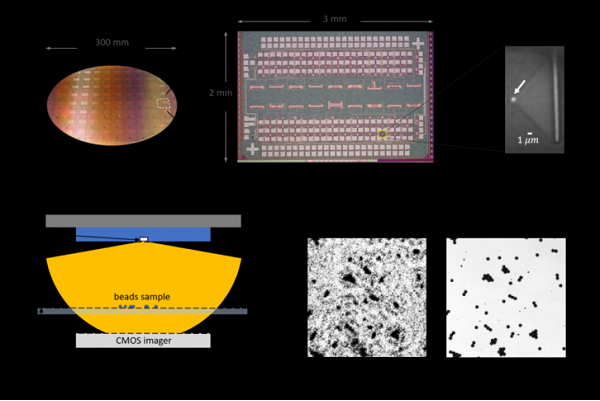
The Singapore-MIT Alliance for Research and Technology (SMART) has developed the world’s smallest silicon LED, measuring less than a micrometre wide. This size innovation allows the placement of the LED directly onto a photonic chip, which opens up a number of potential new avenues to be explored.
To mimic a real-world application of the new technology, the researchers integrated their tiny LED into a lensless holographic microscope. The result was a lensless microscope that produces more accurate high-resolution images than a traditional optical microscope, with a resolution of 20 microns, roughly the length of a human skin cell.
ADVERTISEMENT
What’s more, since this same type of silicon chip makes up the “eye” of modern smartphones, this technology could be easily placed into a smartphone, turning the average phone into a high-resolution microscope.
“On top of its immense potential in lensless holography, our new LED has a wide range of other possible applications,” an author of the study, Rajeev Ram, says.
“Because its wavelength is within the minimum absorption window of biological tissues, together with its high intensity and nanoscale emission area, our LED could be ideal for bio-imaging and bio-sensing applications, including near-field microscopy and implantable CMOS devices.”
-
ADVERTISEMENT
-
ADVERTISEMENT
-
ADVERTISEMENT
-
ADVERTISEMENT